[info] Power supply - kb1gtt

Hardware inside and outside of the ECU
Post Reply
Rhinoman
contributor
contributor
Posts: 256
Joined: Thu Sep 24, 2015 2:14 pm
Location: Wiltshire, UK

Re: My observations on Frankenso 0.4

Post by Rhinoman »

I'll start with the PSU:

Image

ISO16750-2 has two specs for load dump, pulse 5b which (from memory) is 45Vpk up to 450ms or pulse 5a which is 113V for up to 400ms. The source impedance is specified as 0.5 to 4 Ohms. The pulse 5a is an exponential rise and fall from the nominal voltage, ie 12V + 101V, pulse 5b is supposed to represent a load dump on a vehicle with a clamped alternator so its the same waveform but clamped at 45V.
In the existing design the front end components are a 20V FET and two 20V Zeners, during a load dump the voltage across the FET would be in the region of 113V - 25V which it isn't going to like. The max current draw is going to be around 80A through a 0.5 Ohm source impedance which is likely to let out the smoke.
The conventional way to deal with this is to use a reasonable sized TVS around 27-36V on the front end with a reasonable sized 50V cap to slew the rise time a little. Reverse voltage protection relies on the TVS conducting in the reverse direction and blowing the main fuse; this is usually the simplest and cheapest option.
Internal fuses are not accepted by the vehicle manufacturers because they don't want anyone opening the ECU and they aren't usually required.
Most ECUs now use a switcher but the ones that I have been involved with switch at around 7.5V and then follow that with a 5V LDO regulator to remove a lot of the switching noise and ripple and an additional advantage would be that the 7.5V could be taken off via an LC filter to power the op-amps.

To test load dump I've used a modified 2kw audio amplifier driven by an arbitrary waveform generator.
User avatar
kb1gtt
contributor
contributor
Posts: 3777
Joined: Tue Sep 10, 2013 1:42 am
Location: ME of USA

Re: Power supply - kb1gtt

Post by kb1gtt »

Great feed back, and thanks. Don't worry so much about the feeling of being critical, I generally look for content before emotion. What doesn't kill it will only make it stronger.

As a quick note on the history of Frankenso and Frankenstein boards. We originally developed several small boards which we eventually smashed together to make the Frankenstein board. AKA it was our baby made from various bits and pieces, as well it often plays nice with replacing sections. Then Frankenso was the same thing as Frankenstein but for a Denso based system. This power supply is one of the sub circuits used on these other Frank series boards.

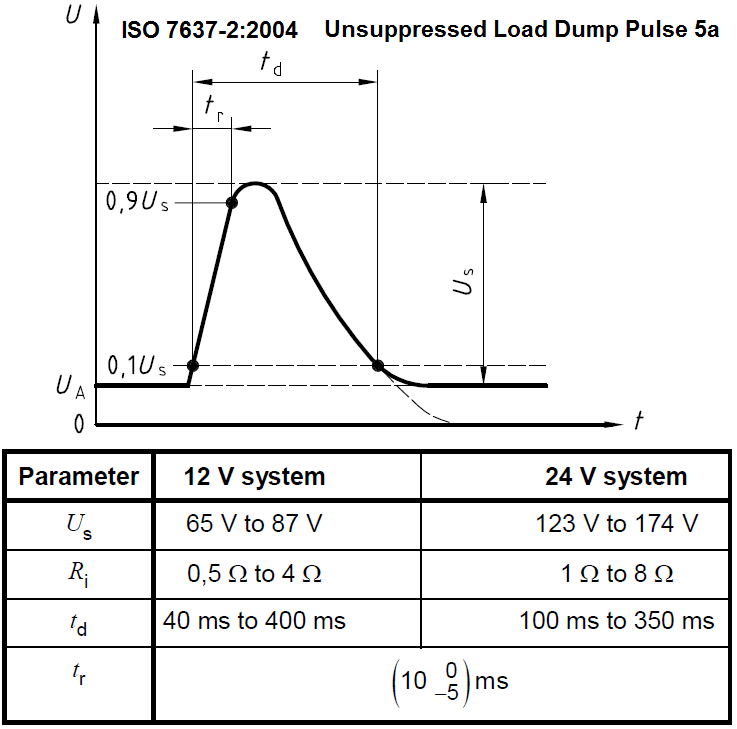
I was not aware of ISO16750-2. I just added it to the wiki. http://rusefi.com/wiki/index.php?title=Manual:Hardware

I have found a PDF copy of the 2006 spec here http://static.ednchina.com/mcu/2009/11/6/2f9e7f31-3753-49a5-b3cc-e9b25fb072a3.pdf which has been attached. Hmmm, that seems to have an IHS copyright note on it, so this link may need to go away. This copy from 2003 doesn't have that copyright note. http://i01.yizimg.com/upload/175936/200793211156599229307.pdf I didn't find the 100v-ish pulse specs in this standard. There are similar specs in 7637-2. Last I recall 7637-2 specified the surge pulse, but didn't specify how often, or for how long it had to sustain. However I'm also working off random bits found on the interwebs, so I might not have the full spec.

Also I found this http://www.vishay.com/docs/49748/49748.pdf which has lots of great scope traces and information that I find interesting.

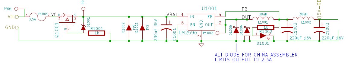
I agree the TVS diodes are undersized, and should be changed for larger ones. They are thru hole components and larger ones should be easy to install, I just haven't gotten around to finding the ones should be used. I haven't figured out which ones as I didn't have a good spec for what kinds of surging I should expect. As well there should be an upstream RF snubber which effects how much energy these clamping diodes would see. What's in there now was based on easy to obtain low cost china parts which would likely "work" for a large single surge, but would not survive sustained surges happening every ?? seconds. I don't have proper facilities to test it, so it has been a step in the right direction, but is probably a weak design. It's better than nothing, but it also really isn't 100% correct.

Do you have a suggested schematic or parts list for the audio amplifier circuit? It would be handy if I had some kind of test fixture to do better testing. There are several ripple rejection signals I would like to test.

I also agree it should have some RF choking that helps keep the fast transients off the PCB. I was hoping to use a thru hole resistor, as a fuse / RF choke, but have done a bunch of testing and found that this is not likely to work. With my DSOquad, I did a sweep of several different wire wound resistors and found that under 100kHz they just don't have the RF blocking inductance required to choke off the RF. The program for the DSOquad is linked here http://essentialscrap.com/dsoquad/freq.html I've been looking at replacing F1 with something like this https://octopart.com/elc-18b470l-panasonic-392391 I'd like to find an inductor that will burn up before some down stream short burns up a PCB trace or something like that.

About the on-board fuse. We expect that there will be an upstream fuse that's smaller and will blow before this fuse blows. I agree that under these surge conditions it should not blow the fuse. However the design now would blow the fuse under several 12V surge conditions. This is better than blowing the MCU or burning a trace on the PCB, but it's also not as good as I would like it to be. We also don't have the quality control systems in place like an OEM. This fuse is partly designed to protect the board when someone doesn't provide proper fusing up steam. Basically if the board was going to go up in flames any how, it would be nice if those flames happened in a place that was easily replaced. Keep in mind that we do not have control over random peoples install practices, while an OEM can ensure that things like a proper up stream fuse has been installed.

Take note there is this file for frankenso https://sourceforge.net/p/rusefi/code/HEAD/tree/trunk/hardware/frankenso/known_issues.txt which list pretty much every item that someone has commented to me. There are some things that haven't been addressed, and many that have been addressed. If you see something you think should be addressed feel free to post a suggested addition to that list. I work on this stuff in 10 minute windows of time, I use that list to remind me what to look at when I get those short windows where I can work on it. Right now the RF choke and fuse blowing issue are triggered by this entry.

Code: Select all

69)                   Change F1 to a wire wound resistor which will also be the weak link and act like a fuse before the PCB breaks, while also snubbing RF
Well that's my 10 minutes for this morning. Welcome along and feel free to comment and make suggestions.
You do not have the required permissions to view the files attached to this post.
Welcome to the friendlier side of internet crazy :)
User avatar
kb1gtt
contributor
contributor
Posts: 3777
Joined: Tue Sep 10, 2013 1:42 am
Location: ME of USA

Re: Power supply - kb1gtt

Post by kb1gtt »

I'm started looking at the surge with QUCS. I'm trying to find a solution that will work with out blowing the fuse. So far it either generates 10+ watts of heat or blows the upstream fuse. These 0.4S make the RF snubbers pretty much non effective. This PDF https://www.maximintegrated.com/en/app-notes/index.mvp/id/4240 pretty much say's you need active clamping to meet these specs. It also separates between high energy surge and low energy surge. AKA relay is a low energy surge, wonky alternator circuit that generates excessive voltage which would be a large energy surge. It notes that the clamping diodes will blow the fuse on a large energy surge. I'd like to find specs for a low energy surge.

https://sourceforge.net/p/daecu/code/HEAD/tree/Hardware/trunk/simulations/12V_Power_Surge/
You do not have the required permissions to view the files attached to this post.
Welcome to the friendlier side of internet crazy :)
User avatar
kb1gtt
contributor
contributor
Posts: 3777
Joined: Tue Sep 10, 2013 1:42 am
Location: ME of USA

Re: Power supply - kb1gtt

Post by kb1gtt »

Hmmm, what about using a high side MOSFET, that opens when the voltage goes higher than desired, or switches in a large resistor to snub the voltage seen by the regulator.
Welcome to the friendlier side of internet crazy :)
User avatar
kb1gtt
contributor
contributor
Posts: 3777
Joined: Tue Sep 10, 2013 1:42 am
Location: ME of USA

Re: Power supply - kb1gtt

Post by kb1gtt »

Looks like there are many active clamp typologies out there. On Frankenso, I'm a bit tight on space, and have kind of backed myself into a corner. Rumble groan moan. I've ready many articles about how this happens.

Any how, it seems a depletion mode N channel MOSFET is among the smallest and simplest to implement. However a bit pricey as it exceeds the regulator cost by about 3X and these kinds of MOSFET's tend to go obsolete on a regular-ish basis. So it has a high probably of needing to find an equiv part in the next couple of years. Any how, it's among the lowest cost options, so I think the below is the way to go. In our case we aren't using the linear, and I plan to be clamping to a higher voltage, but this provides the basic concept.
N-MOSFET_Depletion_Clamp.PNG
Source of that graphic found here
http://ww1.microchip.com/downloads/en/AppNotes/AN-D66.pdf

These MOSFET's could be suitable, but cost about $6 which is kind of blah pricing, but better than blowing the fuse when you hit a surge. These are greater than 150V rated, greater than 5A continuous conduction, N-channel depletion mode MOSFET's.
http://www.digikey.com/product-detail/en/IXTA6N50D2/IXTA6N50D2-ND/2183277
http://www.digikey.com/product-detail/en/IXTP6N50D2/IXTP6N50D2-ND/2183261

Perhaps worth nothing, that most datasheets don't specify enhanced mode vs depletion mode in the searchable text. Enhanced mode is most common, so that's what you'll typically get. The datasheets typically tell you, but they commonly do it graphically. See "MOSFET dep" on this wiki page. It's kind of a pain as you can't specify to google that you want the graphic with a solid line and arrow in the middle, as opposed to dashed line and arrow in the middle. Also these graphics aren't very consistent either. As the datahsheets on the above noted depletion mode MOSFET's show the graphic that wikipedia notes as enhanced mode. It's probably a typo / wrong graphic on the datasheet. Point being that finding a depletion mode is a kind of a pain.

https://en.wikipedia.org/wiki/MOSFET#Circuit_symbols
You do not have the required permissions to view the files attached to this post.
Welcome to the friendlier side of internet crazy :)
User avatar
kb1gtt
contributor
contributor
Posts: 3777
Joined: Tue Sep 10, 2013 1:42 am
Location: ME of USA

Re: Power supply - kb1gtt

Post by kb1gtt »

This PDF notes several chips with various current capabilities. http://www.ixyspower.com/images/literature/500V-1000V_Depletion_Mode_D2tm.pdf as well it notes that N-channel depletion mode MOSFET topology is good for automotive applications. I see the 0.8A device is under $2 and the 6A device is about $6. I also found this https://octopart.com/cpc3703ctr-ixys-22614848 which is under $1 for 350mA.

Page 8 of this PDF provides some math for how to select the MOSFET http://www.ixysic.com/home/pdfs.nsf/www/AN-500.pdf/$file/AN-500.pdf

I think I'm going to plan for the 5A to 6A device, but also add the smaller 350mA package, such that someone can choose low current for lower $, but I think the primary plan should be for the higher current as we offer the 5V for powering stuff on the CANbus connector. That 5V can potentially need higher current.

Unless someone comments, I'm going to plan for these two parts http://datasheet.octopart.com/CPC3703CTR-IXYS-datasheet-24914314.pdf or http://ixdev.ixys.com/DataSheet/DS100177B(IXTA-TP-TH6N50D2).pdf
Welcome to the friendlier side of internet crazy :)
User avatar
kb1gtt
contributor
contributor
Posts: 3777
Joined: Tue Sep 10, 2013 1:42 am
Location: ME of USA

Re: Power supply - kb1gtt

Post by kb1gtt »

This is what I'm currently thinking will prevent the fuse blowing when you have a sustained 100V surge voltage on the 14V power lines. I still have to do some checks, like making sure the gate voltage is OK as the drain and source get pulled away from the GND / 14V voltages. But this should be pretty close to a functional design. Q1002 is a depletion mode (Normally closed) N channel MOSFET. D1002 would need to change to a 15.5V TVS, as the MOSFET has a max 4.5V gate voltage.

Hmmm, I probably should add current limiting resistor like R1001. Any how, this is a start.
You do not have the required permissions to view the files attached to this post.
Welcome to the friendlier side of internet crazy :)
Rhinoman
contributor
contributor
Posts: 256
Joined: Thu Sep 24, 2015 2:14 pm
Location: Wiltshire, UK

Re: Power supply - kb1gtt

Post by Rhinoman »

ISO 7637-2 is obsolete and was replaced by ISO 16750-2 which was updated with the tests from 7637, the ISO specs are all subject to stringent copyright conditions but there are copies available on the net. I think that you need a version from 2010 onwards but the Vishay document is a good reference.
The 100V pulse comes from the load dump pulse 5A:

Image

The exact values that are needed are usually specified by the vehicle manufacturer because they are mostly dependent on the alternator used. For a generic ECU you would need to take the worst case values, i.e. 0.5R, 87V and 400ms.

From memory Ua is 12V because the test is intended to replicate a jump start with the jump leads removed with the battery still flat so the peak voltage, worst case, would be 12+87 = 99V.
The energy that needs to be dissipated is equivalent to the area under the curve so the higher the clamping voltage the lower the energy. The LM2596 is a 40V device so you would need something like an SMBJ24A which has a 'maximum' datasheet clamping voltage of 38.9V, which is similar to the device specified in the Vishay document. I should have a simulation that will calculate the energy. The filter caps on the input to the switcher would need to be 50V and they should really be part of an LC filter to the switcher as well to reduce the switching noise appearing on the supply.

Usually the system fuse would be a 10a or 15A device, you really need to specify the type as their characteristics do vary. The fuse is primarily to protect the wiring only, not any modules which should have their own protection circuitry. You need to look at the time-current characteristics as well as the temperature de-rating curve to determine how long it will take the fuse to blow - its not the current that blows the fuse but the heat/power dissipation. The specs for an ATO blade fuse are given here:

http://www.littelfuse.com/~/media/automotive/datasheets/fuses/passenger-car-and-commercial-vehicle/blade-fuses/littelfuse_ato_blade_fuses.pdf

With a 0.5 Ohm source impedance then the maximum current will be approximately 100 - 9/0.5 = 120A, in reality the clamping time is going to be maybe 200ms, 120A for 200ms is 24A but you only get 120A for a very short duration so the real average will be a fair bit less than that; I will see if I can find my simulation to get a more accurate figure.
If you want to avoid the fuse blowing during a reverse battery connection, which isn't usually a requirement then you can use a bi-directional TVS and have the reverse blocking transistor after the clamping circuit. However, if the worst consequence of a reverse battery connection is a blown fuse then most mechanics would be very relieved.
Rhinoman
contributor
contributor
Posts: 256
Joined: Thu Sep 24, 2015 2:14 pm
Location: Wiltshire, UK

Re: Power supply - kb1gtt

Post by Rhinoman »

The amplifier was a commercial amp made by Crown and it is old and very heavy!
User avatar
kb1gtt
contributor
contributor
Posts: 3777
Joined: Tue Sep 10, 2013 1:42 am
Location: ME of USA

Re: Power supply - kb1gtt

Post by kb1gtt »

Do you have thoughts about the active clamping with a n-channel depletion mode MOSFET? I like this as it can sustain a 150V continuous surge indefinitely. It may cost a couple pennies more than the having a TVS clamp that is tuned to not blow the fuse, but we also have low qty so it's not really a huge pile of $. As well it doesn't clamp the voltage but steps it down to a safe level. Hmmm, looks like the above graphic is a bit out of date. I now have a bias pull up resistor on a 15V zener such that the Q1002 will clamp at 18V. I have some QUCS pictures and updated schematic to share this evening.

I'd also like to find a better p-mosfet. The one we have is only there because it was what the china assembler had on hand. I'd like to find a P-MOSFET that's pin compatible, 5A friendly, low Rds, alternative that's more like 40V or more capable. I don't like having the active clamp set to 18V. I feel it's to close to normal operation.

I agree when selecting a fuse you need to look at the datasheet, especially the I2T specs. These surges events often fatigue the fuse and cause nuisance trips when you exceed the I2T specs. If you size it correctly, they can last for a very long time, but often people don't look at the I2T ratings.
Welcome to the friendlier side of internet crazy :)
User avatar
kb1gtt
contributor
contributor
Posts: 3777
Joined: Tue Sep 10, 2013 1:42 am
Location: ME of USA

Re: Power supply - kb1gtt

Post by kb1gtt »

This is the current schematic and simulation. I'm almost tempted to remove the original TVS diode(s), but might as well leave it there for some extra protection. It shows that with a 100V pulse, the regulator only ever see's 18V to 19V. It also shows that the limiting factor will be thermal, as the MOSFET would have to absorb a peak of 11 watts under normal ECU loading, and if you are running 5A on the 5V, the MOSFET would need to absorb a peak of 400W. The specs I've found indicate a surge once a minute for 10 minutes. With the DPAK, this should have a low enough thermal resistance to the heat sink to prevent over heating. However if your alternator or something goes continuously wonky, it would potentially hit a thermal limit as some point. Either way, it appears we have a solution that would prevent the blowing the fuse upon a load dump.
You do not have the required permissions to view the files attached to this post.
Welcome to the friendlier side of internet crazy :)
User avatar
AndreyB
Site Admin
Posts: 14727
Joined: Wed Aug 28, 2013 1:28 am
Location: Jersey City
Github Username: rusefillc
Slack: Andrey B

Re: Power supply - kb1gtt

Post by AndreyB »

This is all magic, it's amazing that the magic is moving forward :)
Very limited telepathic abilities - please post logs & tunes where appropriate - http://rusefi.com/s/questions

Always looking for C/C++/Java/PHP developers! Please help us see https://rusefi.com/s/howtocontribute
User avatar
kb1gtt
contributor
contributor
Posts: 3777
Joined: Tue Sep 10, 2013 1:42 am
Location: ME of USA

Re: Power supply - kb1gtt

Post by kb1gtt »

Updated schematic and layout posted which includes the active surge suppression protection. This should handle multiple surges up to 150V. The key limitation will be how hot it can get. That's something I won't know until it's Rth is measured.
Welcome to the friendlier side of internet crazy :)
Rhinoman
contributor
contributor
Posts: 256
Joined: Thu Sep 24, 2015 2:14 pm
Location: Wiltshire, UK

Re: Power supply - kb1gtt

Post by Rhinoman »

kb1gtt wrote:The specs I've found indicate a surge once a minute for 10 minutes.
That's the minimum requirement, most manufacturers spec that but the last ECU that I did was 100 repetitions - in reality the power dissipation stabilises long before you get to the end of that test.
Active clamping should work but at that cost it would never make it into a production ECU. A lot of the information you will find on line is not really targeted at engine management, there are a lot of other modules that drive stuff like air-con and power windows have a very low current draw on the 5V.
User avatar
kb1gtt
contributor
contributor
Posts: 3777
Joined: Tue Sep 10, 2013 1:42 am
Location: ME of USA

Re: Power supply - kb1gtt

Post by kb1gtt »

How I wish I had the resources to put into designing this with a non-active design. To properly do this with a non active TVS diode design, you need to specify the upstream fuse, then test your design against that fuse. I don't have the test equipment, budget, or time resources to dedicate to spinning a board, then testing it until it's likely destruction. I wish I did have those resources and time, but life takes priority over the hobby.

In our case we have 16 engines, and I believe we expect to be low qty for the foreseeable future. The 5A friendly clamping MOSFET costs about $6, and the 300mA clamping MOSFET costs about $0.80 in qty 1. A TVS diode would be around $0.60. I agree this is pricey, especially if thinking qty, and the active design would likely be changed if an order were pursued to make some kind of significant qty. Until qty's are significant, the cash outlay is very small.

I look at it like this, if I can pay $6 more on a system that costs hundreds, and it means I can guarantee that I don't pop a fuse when the head light blows, I'd be willing to pay that extra couple bucks. If someone is concerned and doesn't expect the 5A, they can save about $5 and use the smaller MOSFET. If I had the resources and time, I'd be all for testing a non active design and honing it down until it is proven to work, but with the lack of resources I have to increase the costs a bit, making sure it will work with less testing.

The active design is limited by the heat sinks thermal characteristics, which are currently unknown. It is very likely that with a proper heat sink this can sustain a continuous 100V spike. At this point I am very confident it will easily survive 100 repetitions at 1 minute spacing's. However until I can test the thermal resistance, that's difficult to know for certain.

Have you seen the updated R0.5? See page 9 of the updated PDF found here https://sourceforge.net/p/rusefi/code/HEAD/tree/trunk/hardware/frankenso/frankenso_schematic.pdf?format=raw
Welcome to the friendlier side of internet crazy :)
Rhinoman
contributor
contributor
Posts: 256
Joined: Thu Sep 24, 2015 2:14 pm
Location: Wiltshire, UK

Re: Power supply - kb1gtt

Post by Rhinoman »

I haven't had any time recently to look at this, I have started assembling my PCB though. You are only going to get a load dump with a battery disconnect, it won't happen through something trivial like a headlight bulb blowing, its almost always caused when a jump start is carried out and the leads are removed with the battery still flat, at that point the alternator is under full load and it takes a period of time for the regulator to compensate for the reduced load. 'll have a look through my files later and see if I have a load dump model. Do you need 5A? its a lot for a 5V supply, other than the micro and a few low current sensors there tends not to be a lot on it. I would have thought that 1A would be more than adequate for internal supplies with a 250mA tracking regulator for external 5V power. The tracking regulator gives short circuit protection and prevents the internal supply from being pulled down in the event of an external short. There isn't much that you can do to calculate thermal characteristics, really you need to create a PCB with the footprint on it and then put a fixed current through the device and measure the temperature rise.
Have you modelled the battery current? you will need some higher frequency decoupling on the input to reduce conducted emissions from the switcher, usually with a switcher you would have an LC pre-filter, I would fit a couple of ceramic caps at least. I may look at that later, I have some 'real work' to do first.
User avatar
kb1gtt
contributor
contributor
Posts: 3777
Joined: Tue Sep 10, 2013 1:42 am
Location: ME of USA

Re: Power supply - kb1gtt

Post by kb1gtt »

I have only done some basic testing, with basic equipment on PCB's that were in the scratch and dent category. I posted about it here http://rusefi.com/forum/viewtopic.php?f=4&t=569&start=168

At some point I should probably connect my hameg spectrum analyzer, but haven't gotten around to doing that yet. The energy above 150kHz on the 12V side is not measurable via my DSO quad, which means it's below about 5mV. Then according to the chart found here http://www.dipolnet.com/conversion_table_-_dbuv_to_uv-mv_bib04.htm 5mV is 74dbuV, so we are somewhere below 74dbuV. I found the below graphic, which shows that some were below 74dbuV is in the realm of OK conducted emissions. I'm not sure how well we are doing, but we should be close to acceptable EMC limits.
73803-fig-4.gif
Graphic originally found here http://electronicdesign.com/energy/understanding-emi-noise-power-system-design

The 5A thing is partly because we can over kill it for reasonably low $, and partly because we don't know what people might connect to the CAN 5V connector. See P401 on page 4 of the frankenso schematic.

That real work thing. Puts food in the mouth but keeps getting in the way of fun work. I've also been plagued with the real work issue.
You do not have the required permissions to view the files attached to this post.
Welcome to the friendlier side of internet crazy :)
Rhinoman
contributor
contributor
Posts: 256
Joined: Thu Sep 24, 2015 2:14 pm
Location: Wiltshire, UK

Re: Power supply - kb1gtt

Post by Rhinoman »

I've never had any luck trying to do this sort of test with a scope, usually they use FFT which isn't really suitable, the spectrum analyser will be much more useful, unfortunately its not something that I personally own. The automotive tests are ISO11452 and CISPR 25 which mandate the use of a LISN to reproduce the automotive environment, that will put an impedance in series with the supply which will affect the results, the also specify the sampling rates for different frequency bands; in my experience you would not pass with that circuit. I have a number of jobs to complete in the next few days, hopefully next week I will be able to contribute something more positive.
User avatar
kb1gtt
contributor
contributor
Posts: 3777
Joined: Tue Sep 10, 2013 1:42 am
Location: ME of USA

Re: Power supply - kb1gtt

Post by kb1gtt »

If you can tell me the LISN impedance I might be able to do the test. I personally have this spectrum analyzer http://www.testequipmentdepot.com/hameg/spectrumanalyzers/hm5012and5014.htm as well I have access to other spectrum analyzers and such at work.

I agree a FFT on a dirt cheap scope is not the proper way to do this test. My concerns with EMC and this circuit aren't under it's normal operation modes, my concerns would be at the point where the MOSFET starts to clamp the voltage, it's a high gain device and it might cause some noise there. AKA noise might happen during a surge event, and EMC technically doesn't allow out of band noise under any conditions. I don't know if it would generate some noise or not, but it could. When it's not clamping, it's not doing anything, so it wouldn't have any real issues there. I'm fairly confident it would pass EMC during normal operation, but with out doing some tests I don't really know what it would do.
Welcome to the friendlier side of internet crazy :)
Rhinoman
contributor
contributor
Posts: 256
Joined: Thu Sep 24, 2015 2:14 pm
Location: Wiltshire, UK

Re: Power supply - kb1gtt

Post by Rhinoman »

I don't see any high-frequency decoupling on the 12V supply, it looks like the 12V only goes to the switcher.
User avatar
kb1gtt
contributor
contributor
Posts: 3777
Joined: Tue Sep 10, 2013 1:42 am
Location: ME of USA

Re: Power supply - kb1gtt

Post by kb1gtt »

Correct there is no high frequency decoupling at the 12V power supply. The switcher has a switching frequency in the kHz range. I followed the MFG's suggested caps and suggested ESR's. The high frequency stuff has decoupling caps at the sources like MCU's other such chips. The DSO Quad goes up to 72MHz and sees less than 5mV of high frequency ripple. 5mV is the minimum the Quad can see. What ever it has, if any, is below what the quad can see.
Welcome to the friendlier side of internet crazy :)
Rhinoman
contributor
contributor
Posts: 256
Joined: Thu Sep 24, 2015 2:14 pm
Location: Wiltshire, UK

Re: Power supply - kb1gtt

Post by Rhinoman »

I'm concerned that you will get a lot of common mode noise because of the amount of current switching on the ground side. The manufacturers recommendations are only a guide, they aren't application specific. Are you measuring in a vehicle with the engine running? have you measured the voltage drop between the ECU ground and the vehicle body?
Rhinoman
contributor
contributor
Posts: 256
Joined: Thu Sep 24, 2015 2:14 pm
Location: Wiltshire, UK

Re: Power supply - kb1gtt

Post by Rhinoman »

There is an application note from National Semiconductor that discusses input filters for switched mode regulators, its dated 2010 but there was an earlier version that I referred to for a switcher that I had in an automotive design.

http://www.ti.com/lit/an/snva538/snva538.pdf

I did discuss this with Michele Sclocchi at the time, it was probably around 2008, and I was supplied with the Mathcad files.
User avatar
kb1gtt
contributor
contributor
Posts: 3777
Joined: Tue Sep 10, 2013 1:42 am
Location: ME of USA

Re: Power supply - kb1gtt

Post by kb1gtt »

Nice article. Thanks for posting it. I'm absorbing it now.

I'd like to replicate the simulation equation they note which appears it was done in MathCad, I wonder if that can be done in a free tool. I don't have MathCAD and I believe it is a paid for program. I suspect the equation can be plugged into SCILabs or similar, but I'm not sure how.

The example uses an 87uF cap, we have a 330uF cap. I believe that's going to drop our front end impedance significantly, but who knows as the larger cap is likely adding more circular / inductive bits with the electrolytic cap. I also don't understand why they have a near DC impedance of 25 ohms. I suspect they had a 25 ohm resistance up stream, which is not shown in the example schematic. I expect the typical 12V battery to be in the mOhm range, and the wire to be significantly sized such that it doesn't have that kind of resistance. I should probably note on the schematic that I expect a minimum of 18awg for the 12V+ wire (that's about .13ohms for 10 ft) with a GND conductor that's minimum 16awg. I think we have a much lower front end impedance than what is shown in that PDF.

I expect the ECU to have it's own GND wire running to the battery. Frame GND's are not friendly. I should probably add a note to the schematic. Keep in mind you will get many issues if you have around .1 ohm to .01 ohms of resistance on your GND leads. Also remember such low resistances are hard to identify with a normal DMM which only has a chance of measuring 1 to 5 ohms.
Welcome to the friendlier side of internet crazy :)
User avatar
kb1gtt
contributor
contributor
Posts: 3777
Joined: Tue Sep 10, 2013 1:42 am
Location: ME of USA

Re: Power supply - kb1gtt

Post by kb1gtt »

I didn't know about TI's WebBench simulation. I ran the simulation, and was surprised they had all but one of the components in the component libraries. The only thing I had to kind of guess at was the inductor, and they appear to have one that was really close to what we have been using, but from a different MFG, so this simulation is likely very good. Also some of the claimed efficiency and such data points match with things I've posted. So that seems like a good real world validation.

This is the PDF copy of the simulation which includes graphs noting an efficiency between 79% at .25A and a peak efficiency at 1.25A of about 85%. As well it notes the average input current is under 1.5A. Unfortunately I don't see an input impedance prediction.
https://sourceforge.net/p/daecu/code/HEAD/tree/Hardware/trunk/simulations/LM2596_5V_power_supply/Design_Report_12V%2C14.5v%2C17V_webench_design_1077162_276_721820786.pdf?format=raw

Here is the thermal simulation, which notes the junction temperature is well below the max of 150C when the ambient is 85C. It also notes how many watts each device is dissipating and shows that those devices are below their max temperatures. All in all it shows that it's meeting the design specs, which is showing good things.
https://sourceforge.net/p/daecu/code/HEAD/tree/Hardware/trunk/simulations/LM2596_5V_power_supply/Thermal_85C_ambient_webench_tsim_1077162_276_277452011.pdf?format=raw

I had it in my head that it was good for 5A, but it's only good for 3A. Good thing the notes printed on the PCB have that correct, and match the simulations. So I'll have to remember it's 3A not 5A. I hope my brain fart didn't miss lead anyone.
Welcome to the friendlier side of internet crazy :)
Rhinoman
contributor
contributor
Posts: 256
Joined: Thu Sep 24, 2015 2:14 pm
Location: Wiltshire, UK

Re: Power supply - kb1gtt

Post by Rhinoman »

The pdf shows an input ripple current of 1.5A at an output current of 1.25A, the 'standard' wire length is 2m which would be around 0.08Ohms. that will give you a ripple current of 120mV, on the 12V wire, the ground wire is carrying lots of other currents and those will either add or subtract to the total potential difference, typically you will see around 0.25 to 1V of total ripple, you can measure that with a scope. The electrolytic will deal with some of the low frequency noise but the switcher will generate a lot of noise up to around 10MHz, if you can't see any then there is an issue with either the equipment or the test method. The simulation also relies on the electrolytic being able to cope with over an amp of ripple current which is a lot for a small cap. You also need to consider susceptibility, there is nothing to stop high frequency noise coming into the ECU through the 12V supply line.

I'm sure that I had a demo version of Mathcad at the time. The source impedance increases with frequency up to |Z| = 50R above something like 10MHz, I will find the details on the LISN.
User avatar
kb1gtt
contributor
contributor
Posts: 3777
Joined: Tue Sep 10, 2013 1:42 am
Location: ME of USA

Re: Power supply - kb1gtt

Post by kb1gtt »

I think you are referencing the "IC Ipk" graph on page 2 found here https://sourceforge.net/p/daecu/code/HEAD/tree/Hardware/trunk/simulations/LM2596_5V_power_supply/Design_Report_12V%2C14.5v%2C17V_webench_design_1077162_276_721820786.pdf?format=raw I find this simulation results a bit unclear. I believe that chart is conveying the peak switching current, and that the higher frequency stuff is coming from the cap, and not over the 12V wire. I believe it's the max switching current per page 4 operating value's brief description. However I really don't know what the is really trying to convey. When I tested it I tested it with alligator clips plugged into a bench supply. I'm guessing that's at least 16AWG perhaps 14AWG, and it was perhaps 1M long, so 2M total length including the GND wire back to the supply. In that setup seeing 75mVp-p to 225mVp-p might indicate significant 12V ripple current, or it might indicate my bench supply was a bit soft. I believe that front end of this GPS-3303 has significant capacitance, but I have no idea if it's impedance is close to a 12V battery. I should probably put in a series sense resistor and take some measurements, which I could then use to compare against the PDF simulation.

The LM2596 datasheet draws the switches as transistors, while the impedance matching PDF's example used the LM2675 which shows MOSFET's for those switches. I would expect the transistors slew rate would limit switching frequency well below the MHz range. I would expect potentially higher frequency content from the LM2675. I haven't seen significant frequency content above 1MHz on the quad.
Welcome to the friendlier side of internet crazy :)
User avatar
kb1gtt
contributor
contributor
Posts: 3777
Joined: Tue Sep 10, 2013 1:42 am
Location: ME of USA

Re: Power supply - kb1gtt

Post by kb1gtt »

It appears this Chinese switcher chip is likely a LM2576 marked LM2596. You can see on the a primary switch frequency of about 50kHz as noted in the picture I posted here http://rusefi.com/forum/viewtopic.php?f=4&t=569&start=168 Notice that's 150kHz/div, with the first spike about 1/3 of the first block. I found this claim in comments of the below web page.

http://www.kerrywong.com/2015/07/24/lm2596-dc-dc-converter-module-testing/

I'm tempted to add an inductor location to the power supply input, such that we have a physical place to put such a choke if it's needed. As it stands now I don't have solid indication that it's needed, and I don't know what values to put there if it's needed. Hmmm, how to resolve this concern..... For now I guess I'm reading EMC PDFs about switch mode supplies. I'm currently absorbing this one http://www.ti.com/lit/an/snva489c/snva489c.pdf
Welcome to the friendlier side of internet crazy :)
User avatar
kb1gtt
contributor
contributor
Posts: 3777
Joined: Tue Sep 10, 2013 1:42 am
Location: ME of USA

Re: Power supply - kb1gtt

Post by kb1gtt »

From this link, http://www.eevblog.com/forum/projects/5uh-lisn-for-spectrum-analyzer-emcemi-work/15/ it looks like the LISN is a 5uH device wired as noted in this schematic.
CISPR 16-1-2 5uH Schematic.png
Here's a picture of my conducted emissions probe. However I have no idea if that's 5uH as noted above or not.
probe.JPG
This web page is the closest thing I have to a datasheet.
http://www.solar-emc.com/MIL-STD-461F.html
I guess I can connect that probe and sniff it even if it's not the correct impedance.
You do not have the required permissions to view the files attached to this post.
Welcome to the friendlier side of internet crazy :)
Rhinoman
contributor
contributor
Posts: 256
Joined: Thu Sep 24, 2015 2:14 pm
Location: Wiltshire, UK

Re: Power supply - kb1gtt

Post by Rhinoman »

I came across this today, I haven't looked at it in any detail:

http://www.diodes.com/downloads/9551
Post Reply